

PCB decisions that carry a product from prototype to production.
A product’s performance, reliability and manufacturability are shaped by its PCB specification and production conditions. KAITECH supports PCB manufacturing from prototype through volume production, matching board technology to required density, signal characteristics, form factor and quantity, including multilayer, HDI, RF, flex and rigid-flex options.
Common Challenges
Have you encountered any of these common challenges?
- Manufacturing conditions such as layer count, material, board thickness, copper weight and finish are not fully defined
- Prototype, low-volume and mass-production stages require different balances of lead time, cost and quality
- Feasibility for special boards such as HDI, RF, Flex or Rigid-Flex must be confirmed early
Our Approach
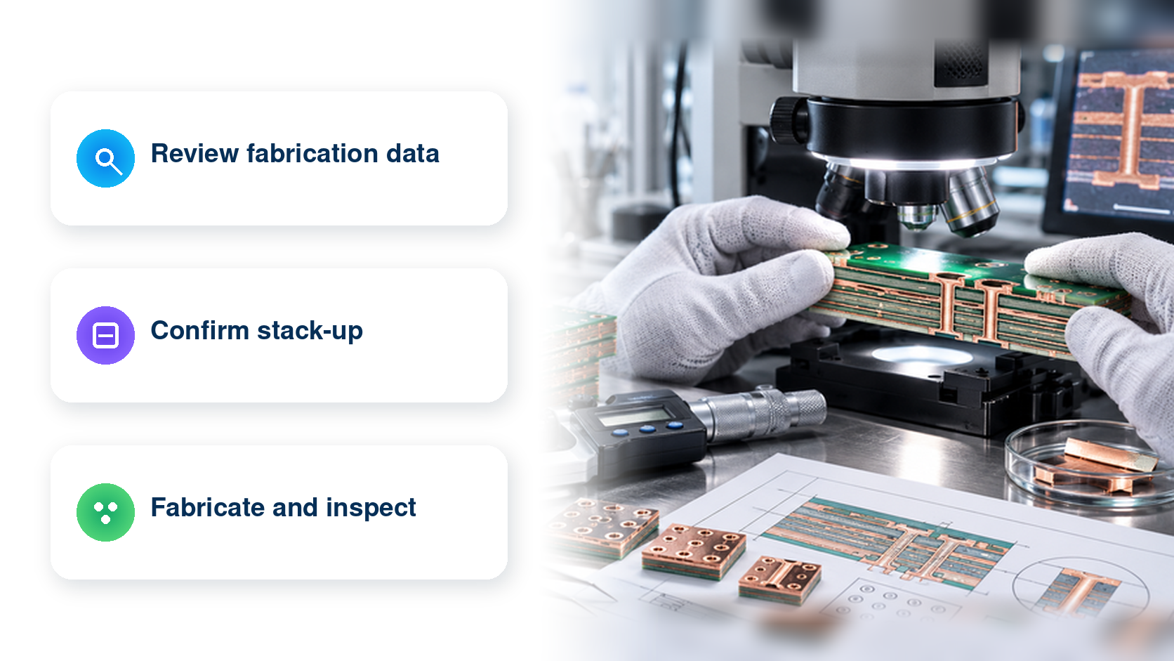
KAITECH reviews the fabrication data, stack-up, materials, dimensions, tolerances, quantity and delivery requirements before production. We help align a practical specification with the application and production stage, including multilayer boards from 2 to 20+ layers and special PCB types. Early review reduces avoidable fabrication changes and keeps the transition from prototype to volume production in view.
What We Deliver
- Manufacturing support for prototype, low-volume and production PCBs
- Multilayer boards from two layers to 20+ layers
- HDI, RF, high-density, flex and rigid-flex PCB options
- Review of manufacturing data such as Gerber files and requirements
- Guidance on materials, thickness, surface finish and panel conditions
We do not treat PCB manufacturing as isolated procurement. The discussion considers components, assembly, testing, embedded software and manufacturability together. Starting from product-level requirements helps clarify the board specification and reduce later rework.
This delivery approach is reflected in our related work. Considering PCB, assembly, embedded software and cloud connectivity together rather than as isolated activities helps expose product requirements earlier and reduces gaps in delivery. We connect discovery, focused validation, implementation and operational adoption rather than treating them as separate phases. Depending on the need, we combine 2-20+ layers, HDI, RF, flex, rigid-flex, Gerber, DFM, surface finishes with the surrounding architecture, selecting technology around the service objective, maintainability and future expansion instead of using a stack for its own sake.
Suitable for IoT devices, measurement equipment, industrial and communication products, consumer electronics, and products moving from prototype to production. From the initial discussion, KAITECH can help you clarify the opportunity, requirements, delivery path and estimate for PCB Manufacturing.